25
views
0
recommends
+1 Recommend
0 collections
    0
    shares
      • Record: found
      • Abstract: found
      • Article: found
      Is Open Access

      Ultrasensitive all-2D MoS 2 phototransistors enabled by an out-of-plane MoS 2 PN homojunction

      research-article
      1 , 1 , 2 ,
      Nature Communications
      Nature Publishing Group UK

      Read this article at

      Bookmark
          There is no author summary for this article yet. Authors can add summaries to their articles on ScienceOpen to make them more accessible to a non-specialist audience.

          Abstract

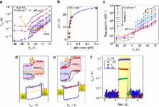
          Two-dimensional transition metal dichalcogenide-based photodetectors have demonstrated potential for the next generation of 2-dimensional optoelectronics. However, to date, their sensitivity has not been superior to that of other technologies. Here we report an ultrasensitive two-dimensional photodetector employing an in-plane phototransistor with an out-of-plane vertical MoS 2 p–n junction as a sensitizing scheme. The vertical built-in field is introduced for the first time in the transport channel of MoS 2 phototransistors by facile chemical surface doping, which separates the photo-excited carriers efficiently and produces a photoconductive gain of >10 5 electrons per photon, external quantum efficiency greater than 10%, responsivity of 7 × 10 4 A W −1, and a time response on the order of tens of ms. This taken together with a very low noise power density yields a record sensitivity with specific detectivity \documentclass[12pt]{minimal} \usepackage{amsmath} \usepackage{wasysym} \usepackage{amsfonts} \usepackage{amssymb} \usepackage{amsbsy} \usepackage{mathrsfs} \usepackage{upgreek} \setlength{\oddsidemargin}{-69pt} \begin{document}$$D^*$$\end{document} of 3.5 × 10 14 Jones in the visible and a broadband response up to 1000 nm.

          Abstract

          Photodetectors based on 2D transition metal dichalcogenides exhibit ever increasingly competitive performance, yet not superior to that of alternative technologies. Here, the authors devise a MoS 2-based phototransistor with an out-of-plane junction, yielding a record detectivity combined with broadband response.

          Related collections

          Most cited references41

          • Record: found
          • Abstract: found
          • Article: found
          Is Open Access

          Atomically thin MoS2: A new direct-gap semiconductor

          The electronic properties of ultrathin crystals of molybdenum disulfide consisting of N = 1, 2, ... 6 S-Mo-S monolayers have been investigated by optical spectroscopy. Through characterization by absorption, photoluminescence, and photoconductivity spectroscopy, we trace the effect of quantum confinement on the material's electronic structure. With decreasing thickness, the indirect band gap, which lies below the direct gap in the bulk material, shifts upwards in energy by more than 0.6 eV. This leads to a crossover to a direct-gap material in the limit of the single monolayer. Unlike the bulk material, the MoS2 monolayer emits light strongly. The freestanding monolayer exhibits an increase in luminescence quantum efficiency by more than a factor of 1000 compared with the bulk material.
            Bookmark
            • Record: found
            • Abstract: found
            • Article: not found

            Strong light-matter interactions in heterostructures of atomically thin films.

            The isolation of various two-dimensional (2D) materials, and the possibility to combine them in vertical stacks, has created a new paradigm in materials science: heterostructures based on 2D crystals. Such a concept has already proven fruitful for a number of electronic applications in the area of ultrathin and flexible devices. Here, we expand the range of such structures to photoactive ones by using semiconducting transition metal dichalcogenides (TMDCs)/graphene stacks. Van Hove singularities in the electronic density of states of TMDC guarantees enhanced light-matter interactions, leading to enhanced photon absorption and electron-hole creation (which are collected in transparent graphene electrodes). This allows development of extremely efficient flexible photovoltaic devices with photoresponsivity above 0.1 ampere per watt (corresponding to an external quantum efficiency of above 30%).
              Bookmark
              • Record: found
              • Abstract: found
              • Article: not found

              High performance multilayer MoS2 transistors with scandium contacts.

              While there has been growing interest in two-dimensional (2-D) crystals other than graphene, evaluating their potential usefulness for electronic applications is still in its infancy due to the lack of a complete picture of their performance potential. The focus of this article is on contacts. We demonstrate that through a proper understanding and design of source/drain contacts and the right choice of number of MoS(2) layers the excellent intrinsic properties of this 2-D material can be harvested. Using scandium contacts on 10-nm-thick exfoliated MoS(2) flakes that are covered by a 15 nm Al(2)O(3) film, high effective mobilities of 700 cm(2)/(V s) are achieved at room temperature. This breakthrough is largely attributed to the fact that we succeeded in eliminating contact resistance effects that limited the device performance in the past unrecognized. In fact, the apparent linear dependence of current on drain voltage had mislead researchers to believe that a truly Ohmic contact had already been achieved, a misconception that we also elucidate in the present article.
                Bookmark

                Author and article information

                Contributors
                Gerasimos.konstantatos@icfo.es
                Journal
                Nat Commun
                Nat Commun
                Nature Communications
                Nature Publishing Group UK (London )
                2041-1723
                18 September 2017
                18 September 2017
                2017
                : 8
                : 572
                Affiliations
                [1 ]GRID grid.473715.3, ICFO—Institut de Ciencies Fotoniques, , The Barcelona Institute of Science and Technology, ; Castelldefels, 08860 Barcelona, Spain
                [2 ]ISNI 0000 0000 9601 989X, GRID grid.425902.8, ICREA—Institució Catalana de Recerca i Estudis Avançats, ; Lluis Companys 23, 08010 Barcelona, Spain
                Article
                722
                10.1038/s41467-017-00722-1
                5603552
                28924234
                dc264edf-e947-41ef-8dc0-9afa51ef8edf
                © The Author(s) 2017

                Open Access This article is licensed under a Creative Commons Attribution 4.0 International License, which permits use, sharing, adaptation, distribution and reproduction in any medium or format, as long as you give appropriate credit to the original author(s) and the source, provide a link to the Creative Commons license, and indicate if changes were made. The images or other third party material in this article are included in the article’s Creative Commons license, unless indicated otherwise in a credit line to the material. If material is not included in the article’s Creative Commons license and your intended use is not permitted by statutory regulation or exceeds the permitted use, you will need to obtain permission directly from the copyright holder. To view a copy of this license, visit http://creativecommons.org/licenses/by/4.0/.

                History
                : 5 May 2017
                : 24 July 2017
                Categories
                Article
                Custom metadata
                © The Author(s) 2017

                Uncategorized
                Uncategorized

                Comments

                Comment on this article