1
views
0
recommends
+1 Recommend
0 collections
    0
    shares
      • Record: found
      • Abstract: found
      • Article: found
      Is Open Access

      Carrier transport and photoconductivity properties of BN 50/NiO 50 nanocomposite films

      research-article

      Read this article at
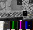
      Bookmark
          There is no author summary for this article yet. Authors can add summaries to their articles on ScienceOpen to make them more accessible to a non-specialist audience.

          Abstract

          BN 50/NiO 50 and Au-loaded BN 50/NiO 50 nanocomposite films were separately fabricated on the glass substrates for carrier transport and photoconductivity properties. X-ray diffraction pattern of the films show the hexagonal structure of BN and presence of defect states by Nelson Riley factor analysis. Morphological images show spherical shaped particles with highly porous structure. The incorporation of NiO may hindered growth of BN layers and resulted in spherical particles. Temperature-dependent conductivity describes semiconductor transport behaviour for deposited nanocomposite films. Thermal activation conduction with low activation energy (∼0.308 eV) may be responsible for the resulting conductivity. Further, the light intensity dependent photoelectrical properties of BN 50/NiO 50 and Au-loaded BN 50/NiO 50 nanocomposites have been explored. The effect of Au nanoparticles loading on enhanced photo-conductivities (∼22% increase) than bare nanocomposite film has been elaborated by proposed mechanism. This study provided the insightful information for carrier transport and photoconductivity of BN-based nanocomposites.

          Related collections

          Most cited references36

          • Record: found
          • Abstract: not found
          • Article: not found

          Surface-Plasmon-Driven Hot Electron Photochemistry

            Bookmark
            • Record: found
            • Abstract: found
            • Article: not found

            Two dimensional hexagonal boron nitride (2D-hBN): synthesis, properties and applications

            Comprehensive summary of the progress including crystal structures, fabrication methods, applications (especially for electronics) and functionalization of 2D-hBN from its discovery. Two dimensional hexagonal boron nitride (2D-hBN), an isomorph of graphene with a very similar layered structure, is uniquely featured by its exotic opto-electrical properties together with mechanical robustness, thermal stability, and chemical inertness. It is thus extensively studied for application in field effect transistors (FETs), tunneling devices, deep UV emitters and detectors, photoelectric devices, and nanofillers. 2D-hBN is considered as one of the most promising materials that can be integrated with other 2D materials, such as graphene and transition metal dichalcogenides (TMDCs), for the next generation microelectronic and other technologies. Although it is by itself an insulator, it can well be tuned by several strategies in terms of properties and functionalities, such as by doping, substitution, functionalization and hybridization, making 2D-hBN a truly versatile type of functional materials for a wide range of applications. In this review, the distinct structural characteristics of 2D-hBN, doping- and defect-induced variations in energy bands and structures, and resultant properties, are presented. There are a wide variety of processing routes that have been developed for 2D-hBN, including also those for doping, substitution, functionalization and combination with other materials to form heterostructures or h-BNC hybrid nanosheets, which are systematically elaborated for novel functions. The comprehensive overview provides the types of the state-of-the-art 2D-hBN made by new synthesis strategies, where the mainstream approaches include exfoliation, chemical vapor deposition, and gas phase epitaxy, together with several other new methods that have been successfully developed in the past few years. On the basis of the extraordinary electrical and functional properties and thermal–mechanical stability, the applications of hBN-based nanosheets as substrates and dielectrics, passivation layers, and nanofillers in nanodevices and nanocomposites are discussed, together with the peculiar optical and wetting characteristics.
              Bookmark
              • Record: found
              • Abstract: found
              • Article: found
              Is Open Access

              Synthesis of large-area multilayer hexagonal boron nitride for high material performance

              Although hexagonal boron nitride (h-BN) is a good candidate for gate-insulating materials by minimizing interaction from substrate, further applications to electronic devices with available two-dimensional semiconductors continue to be limited by flake size. While monolayer h-BN has been synthesized on Pt and Cu foil using chemical vapour deposition (CVD), multilayer h-BN is still absent. Here we use Fe foil and synthesize large-area multilayer h-BN film by CVD with a borazine precursor. These films reveal strong cathodoluminescence and high mechanical strength (Young's modulus: 1.16±0.1 TPa), reminiscent of formation of high-quality h-BN. The CVD-grown graphene on multilayer h-BN film yields a high carrier mobility of ∼24,000 cm2 V−1 s−1 at room temperature, higher than that (∼13,000 2 V−1 s−1) with exfoliated h-BN. By placing additional h-BN on a SiO2/Si substrate for a MoS2 (WSe2) field-effect transistor, the doping effect from gate oxide is minimized and furthermore the mobility is improved by four (150) times.
                Bookmark

                Author and article information

                Contributors
                Journal
                Heliyon
                Heliyon
                Heliyon
                Elsevier
                2405-8440
                18 February 2023
                March 2023
                18 February 2023
                : 9
                : 3
                : e13865
                Affiliations
                [a ]University Centre for Research and Development, Chandigarh University, Mohali, 140413, Punjab, India
                [b ]Department of Chemistry, University Institute of Sciences, Chandigarh University, Mohali, 140413, Punjab, India
                [c ]Centre for Interdisciplinary Research, University of Petroleum and Energy Studies (UPES), Dehradun, 248007, Uttarakhand, India
                [d ]Department of Physics, University Institute of Sciences, Chandigarh University, Mohali, 140413, Punjab, India
                [e ]Advanced Materials Research Lab, Department of Physics, Punjabi University Patiala, 147 002, Punjab, India
                [f ]Department of Physics, Sardar Patel University, Mandi, Himachal Pradesh, 175001, India
                Author notes
                []Corresponding author. akshaykumar.tiet@ 123456gmail.com
                [1]

                Equal Contribution.

                Article
                S2405-8440(23)01072-1 e13865
                10.1016/j.heliyon.2023.e13865
                9982041
                36873537
                c52af8f3-542a-47f8-8a4a-23bd2c004348
                © 2023 The Authors

                This is an open access article under the CC BY-NC-ND license (http://creativecommons.org/licenses/by-nc-nd/4.0/).

                History
                : 3 November 2022
                : 9 February 2023
                : 14 February 2023
                Categories
                Research Article

                nanocomposites,thin films,defects,surface plasmon resonance,photoconductivity

                Comments

                Comment on this article