3
views
0
recommends
+1 Recommend
0 collections
    0
    shares
      • Record: found
      • Abstract: found
      • Article: found
      Is Open Access

      Hot-Carrier Cooling in High-Quality Graphene Is Intrinsically Limited by Optical Phonons

      research-article

      Read this article at

      Bookmark
          There is no author summary for this article yet. Authors can add summaries to their articles on ScienceOpen to make them more accessible to a non-specialist audience.

          Abstract

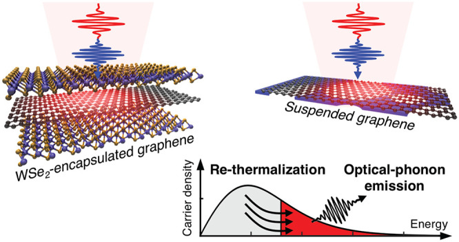
          Many promising optoelectronic devices, such as broadband photodetectors, nonlinear frequency converters, and building blocks for data communication systems, exploit photoexcited charge carriers in graphene. For these systems, it is essential to understand the relaxation dynamics after photoexcitation. These dynamics contain a sub-100 fs thermalization phase, which occurs through carrier–carrier scattering and leads to a carrier distribution with an elevated temperature. This is followed by a picosecond cooling phase, where different phonon systems play a role: graphene acoustic and optical phonons, and substrate phonons. Here, we address the cooling pathway of two technologically relevant systems, both consisting of high-quality graphene with a mobility >10 000 cm 2 V –1 s –1 and environments that do not efficiently take up electronic heat from graphene: WSe 2-encapsulated graphene and suspended graphene. We study the cooling dynamics using ultrafast pump–probe spectroscopy at room temperature. Cooling via disorder-assisted acoustic phonon scattering and out-of-plane heat transfer to substrate phonons is relatively inefficient in these systems, suggesting a cooling time of tens of picoseconds. However, we observe much faster cooling, on a time scale of a few picoseconds. We attribute this to an intrinsic cooling mechanism, where carriers in the high-energy tail of the hot-carrier distribution emit optical phonons. This creates a permanent heat sink, as carriers efficiently rethermalize. We develop a macroscopic model that explains the observed dynamics, where cooling is eventually limited by optical-to-acoustic phonon coupling. These fundamental insights will guide the development of graphene-based optoelectronic devices.

          Related collections

          Most cited references59

          • Record: found
          • Abstract: found
          • Article: not found

          Boron nitride substrates for high-quality graphene electronics

          Graphene devices on standard SiO(2) substrates are highly disordered, exhibiting characteristics that are far inferior to the expected intrinsic properties of graphene. Although suspending the graphene above the substrate leads to a substantial improvement in device quality, this geometry imposes severe limitations on device architecture and functionality. There is a growing need, therefore, to identify dielectrics that allow a substrate-supported geometry while retaining the quality achieved with a suspended sample. Hexagonal boron nitride (h-BN) is an appealing substrate, because it has an atomically smooth surface that is relatively free of dangling bonds and charge traps. It also has a lattice constant similar to that of graphite, and has large optical phonon modes and a large electrical bandgap. Here we report the fabrication and characterization of high-quality exfoliated mono- and bilayer graphene devices on single-crystal h-BN substrates, by using a mechanical transfer process. Graphene devices on h-BN substrates have mobilities and carrier inhomogeneities that are almost an order of magnitude better than devices on SiO(2). These devices also show reduced roughness, intrinsic doping and chemical reactivity. The ability to assemble crystalline layered materials in a controlled way permits the fabrication of graphene devices on other promising dielectrics and allows for the realization of more complex graphene heterostructures.
            Bookmark
            • Record: found
            • Abstract: found
            • Article: not found

            Photodetectors based on graphene, other two-dimensional materials and hybrid systems.

            Graphene and other two-dimensional materials, such as transition metal dichalcogenides, have rapidly established themselves as intriguing building blocks for optoelectronic applications, with a strong focus on various photodetection platforms. The versatility of these material systems enables their application in areas including ultrafast and ultrasensitive detection of light in the ultraviolet, visible, infrared and terahertz frequency ranges. These detectors can be integrated with other photonic components based on the same material, as well as with silicon photonic and electronic technologies. Here, we provide an overview and evaluation of state-of-the-art photodetectors based on graphene, other two-dimensional materials, and hybrid systems based on the combination of different two-dimensional crystals or of two-dimensional crystals and other (nano)materials, such as plasmonic nanoparticles, semiconductors, quantum dots, or their integration with (silicon) waveguides.
              Bookmark
              • Record: found
              • Abstract: found
              • Article: not found

              One-dimensional electrical contact to a two-dimensional material.

              Heterostructures based on layering of two-dimensional (2D) materials such as graphene and hexagonal boron nitride represent a new class of electronic devices. Realizing this potential, however, depends critically on the ability to make high-quality electrical contact. Here, we report a contact geometry in which we metalize only the 1D edge of a 2D graphene layer. In addition to outperforming conventional surface contacts, the edge-contact geometry allows a complete separation of the layer assembly and contact metallization processes. In graphene heterostructures, this enables high electronic performance, including low-temperature ballistic transport over distances longer than 15 micrometers, and room-temperature mobility comparable to the theoretical phonon-scattering limit. The edge-contact geometry provides new design possibilities for multilayered structures of complimentary 2D materials.
                Bookmark

                Author and article information

                Journal
                ACS Nano
                ACS Nano
                nn
                ancac3
                ACS Nano
                American Chemical Society
                1936-0851
                1936-086X
                17 June 2021
                27 July 2021
                : 15
                : 7
                : 11285-11295
                Affiliations
                []NEST, Istituto Nanoscienze-CNR and Scuola Normale Superiore , 56127 Pisa, Italy
                []Department of Physics, Politecnico di Milano , 20133 Milan, Italy
                []Max-Planck-Institut für Polymerforschung , 55128 Mainz, Germany
                [§ ]School of Physics and Astronomy, University of Manchester , M13 9PL Manchester, U.K.
                []Catalan Institute of Nanoscience and Nanotechnology (ICN2), BIST & CSIC , Campus UAB, Bellaterra, Barcelona 08193, Spain
                []JARA-FIT and second Institute of Physics, RWTH Aachen University , 52074 Aachen, Germany, EU
                [# ]Center for Nanochemistry, College of Chemistry and Molecular Engineering, Academy for Advanced Interdisciplinary Studies, Peking University , Beijing 100871, China
                [@ ]Beijing Graphene Institute , Beijing 100095, P. R. China
                []NanoMat/Q-Mat/CESAM, Université de Liège (B5) , B-4000 Liège, Belgium
                []Center for Nanotechnology Innovation IIT@NEST , Piazza San Silvestro 12, 56127 Pisa, Italy
                []ICFO - Institut de Ciències Fotòniques, BIST , Castelldefels, Barcelona 08860, Spain
                []Graphene Laboratories , Via Morego 30, 16163 Genova, Italy
                []ICREA - Institució Catalana de Reçerca i Estudis Avancats , 08010 Barcelona, Spain
                Author notes
                Author information
                https://orcid.org/0000-0003-4779-3549
                https://orcid.org/0000-0002-1855-1287
                https://orcid.org/0000-0002-8150-9743
                https://orcid.org/0000-0002-8134-7633
                https://orcid.org/0000-0001-9764-6120
                https://orcid.org/0000-0001-6851-8453
                https://orcid.org/0000-0003-0940-3984
                https://orcid.org/0000-0003-4630-1776
                https://orcid.org/0000-0003-1569-0238
                https://orcid.org/0000-0003-0065-7988
                https://orcid.org/0000-0002-4958-7362
                https://orcid.org/0000-0002-0055-6231
                Article
                10.1021/acsnano.0c10864
                8320233
                34139125
                94a95017-a74b-4591-b0f0-4286359cb967
                © 2021 The Authors. Published by American Chemical Society

                Permits non-commercial access and re-use, provided that author attribution and integrity are maintained; but does not permit creation of adaptations or other derivative works ( https://creativecommons.org/licenses/by-nc-nd/4.0/).

                History
                : 28 December 2020
                : 03 June 2021
                Funding
                Funded by: Agencia Estatal de Investigación, Ministerio de Ciencia, Innovación y Universidades, doi NA;
                Award ID: CEX2019-000910-S
                Funded by: Fundación Cellex, doi 10.13039/100008050;
                Award ID: NA
                Funded by: Fundació Privada Mir-Puig, doi NA;
                Award ID: NA
                Funded by: European Regional Development Fund, doi 10.13039/501100008530;
                Award ID: NA
                Funded by: Agència de Gestió d''Ajuts Universitaris i de Recerca, doi NA;
                Award ID: 2017SGR1369
                Funded by: Ministerio de Economía y Competitividad, doi 10.13039/501100003329;
                Award ID: PID2019-111673GB-I00
                Funded by: Université de Liège, doi 10.13039/501100005627;
                Award ID: NA
                Funded by: Agencia Estatal de Investigación, Ministerio de Ciencia, Innovación y Universidades, doi NA;
                Award ID: SEV-2017-0706
                Funded by: Generalitat de Catalunya, doi 10.13039/501100002809;
                Award ID: NA
                Funded by: Agencia Estatal de Investigación, Ministerio de Ciencia, Innovación y Universidades, doi NA;
                Award ID: RYC-2017-22330
                Funded by: Max Planck Graduate Center, Johannes Gutenberg-Universität Mainz, doi NA;
                Award ID: NA
                Funded by: Agencia Estatal de Investigación, Ministerio de Ciencia, Innovación y Universidades, doi NA;
                Award ID: PGC2018-096875-BI00
                Funded by: Fonds De La Recherche Scientifique - FNRS, doi 10.13039/501100002661;
                Award ID: T.0103.19-ALPS
                Funded by: National Natural Science Foundation of China, doi 10.13039/501100001809;
                Award ID: 52072042
                Funded by: National Natural Science Foundation of China, doi 10.13039/501100001809;
                Award ID: 51520105003
                Funded by: Leverhulme Trust, doi 10.13039/501100000275;
                Award ID: RPG-2019-363
                Funded by: H2020 Marie SkÃ…?odowska-Curie Actions, doi 10.13039/100010665;
                Award ID: 873028
                Funded by: H2020 Future and Emerging Technologies, doi 10.13039/100010664;
                Award ID: 881603
                Funded by: H2020 European Research Council, doi 10.13039/100010663;
                Award ID: 804349
                Funded by: H2020 European Research Council, doi 10.13039/100010663;
                Award ID: 670949
                Categories
                Article
                Custom metadata
                nn0c10864
                nn0c10864

                Nanotechnology
                graphene,cooling dynamics,hot electrons,transient absorption microscopy,optical phonons,phonon bottleneck

                Comments

                Comment on this article