11
views
0
recommends
+1 Recommend
0 collections
    0
    shares
      • Record: found
      • Abstract: found
      • Article: found
      Is Open Access

      Lead-Free Halide Double Perovskite Materials: A New Superstar Toward Green and Stable Optoelectronic Applications

      review-article

      Read this article at

      Bookmark
          There is no author summary for this article yet. Authors can add summaries to their articles on ScienceOpen to make them more accessible to a non-specialist audience.

          Highlights

          • Lead-based halide perovskite materials have revealed excellent properties in optoelectronic applications. However, the material stability and the toxicity of lead still hinder their large-scale commercial applications.

          • Lead-free halide double perovskite materials possess the characteristics of environmental friendliness, exceptional stability and tunable optoelectronic properties.

          • A limited number of halide double perovskites have been synthesized, and extremely few have been developed for optoelectronic applications. Continuing effort is needed to explore more halide double perovskites and modulate the properties for their further applications.

          Abstract

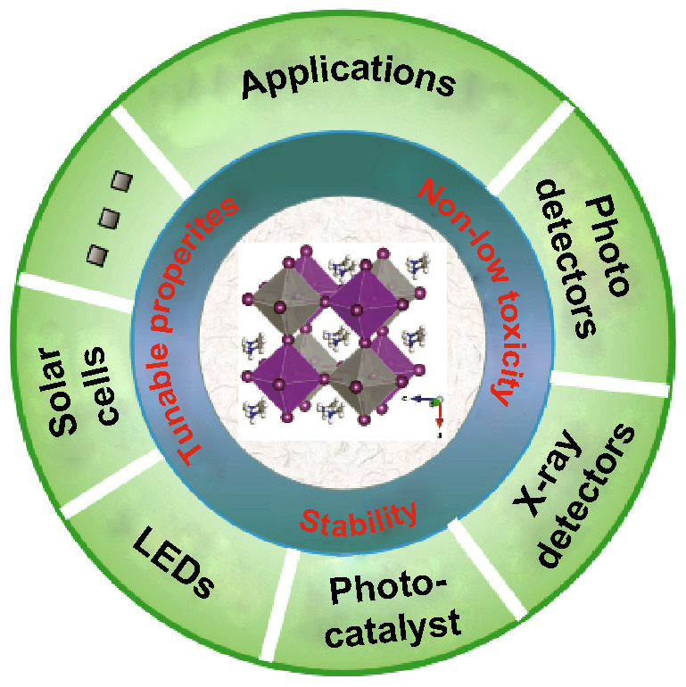
          Lead-based halide perovskites have emerged as excellent semiconductors for a broad range of optoelectronic applications, such as photovoltaics, lighting, lasing and photon detection. However, toxicity of lead and poor stability still represent significant challenges. Fortunately, halide double perovskite materials with formula of A 2M(I)M(III)X 6 or A 2M(IV)X 6 could be potentially regarded as stable and green alternatives for optoelectronic applications, where two divalent lead ions are substituted by combining one monovalent and one trivalent ions, or one tetravalent ion. Here, the article provides an up-to-date review on the developments of halide double perovskite materials and their related optoelectronic applications including photodetectors, X-ray detectors, photocatalyst, light-emitting diodes and solar cells. The synthesized halide double perovskite materials exhibit exceptional stability, and a few possess superior optoelectronic properties. However, the number of synthesized halide double perovskites is limited, and more limited materials have been developed for optoelectronic applications to date. In addition, the band structures and carrier transport properties of the materials are still not desired, and the films still manifest low quality for photovoltaic applications. Therefore, we propose that continuing efforts are needed to develop more halide double perovskites, modulate the properties and grow high-quality films, with the aim of opening the wild practical applications.

          Related collections

          Most cited references106

          • Record: found
          • Abstract: found
          • Article: not found

          Organometal halide perovskites as visible-light sensitizers for photovoltaic cells.

          Two organolead halide perovskite nanocrystals, CH(3)NH(3)PbBr(3) and CH(3)NH(3)PbI(3), were found to efficiently sensitize TiO(2) for visible-light conversion in photoelectrochemical cells. When self-assembled on mesoporous TiO(2) films, the nanocrystalline perovskites exhibit strong band-gap absorptions as semiconductors. The CH(3)NH(3)PbI(3)-based photocell with spectral sensitivity of up to 800 nm yielded a solar energy conversion efficiency of 3.8%. The CH(3)NH(3)PbBr(3)-based cell showed a high photovoltage of 0.96 V with an external quantum conversion efficiency of 65%.
            Bookmark
            • Record: found
            • Abstract: found
            • Article: not found

            Electron-hole diffusion lengths exceeding 1 micrometer in an organometal trihalide perovskite absorber.

            Organic-inorganic perovskites have shown promise as high-performance absorbers in solar cells, first as a coating on a mesoporous metal oxide scaffold and more recently as a solid layer in planar heterojunction architectures. Here, we report transient absorption and photoluminescence-quenching measurements to determine the electron-hole diffusion lengths, diffusion constants, and lifetimes in mixed halide (CH3NH3PbI(3-x)Cl(x)) and triiodide (CH3NH3PbI3) perovskite absorbers. We found that the diffusion lengths are greater than 1 micrometer in the mixed halide perovskite, which is an order of magnitude greater than the absorption depth. In contrast, the triiodide absorber has electron-hole diffusion lengths of ~100 nanometers. These results justify the high efficiency of planar heterojunction perovskite solar cells and identify a critical parameter to optimize for future perovskite absorber development.
              Bookmark
              • Record: found
              • Abstract: found
              • Article: not found

              Efficient hybrid solar cells based on meso-superstructured organometal halide perovskites.

              The energy costs associated with separating tightly bound excitons (photoinduced electron-hole pairs) and extracting free charges from highly disordered low-mobility networks represent fundamental losses for many low-cost photovoltaic technologies. We report a low-cost, solution-processable solar cell, based on a highly crystalline perovskite absorber with intense visible to near-infrared absorptivity, that has a power conversion efficiency of 10.9% in a single-junction device under simulated full sunlight. This "meso-superstructured solar cell" exhibits exceptionally few fundamental energy losses; it can generate open-circuit photovoltages of more than 1.1 volts, despite the relatively narrow absorber band gap of 1.55 electron volts. The functionality arises from the use of mesoporous alumina as an inert scaffold that structures the absorber and forces electrons to reside in and be transported through the perovskite.
                Bookmark

                Author and article information

                Contributors
                yangjp@njupt.edu.cn
                iamxali@njupt.edu.cn
                Journal
                Nanomicro Lett
                Nanomicro Lett
                Nano-Micro Letters
                Springer Singapore (Singapore )
                2311-6706
                2150-5551
                27 February 2019
                27 February 2019
                December 2019
                : 11
                : 16
                Affiliations
                [1 ]ISNI 0000 0004 0369 3615, GRID grid.453246.2, New Energy Technology Engineering Laboratory of Jiangsu Province & School of Science, , Nanjing University of Posts and Telecommunications (NJUPT), ; Nanjing, 210023 People’s Republic of China
                [2 ]ISNI 0000 0004 0369 3615, GRID grid.453246.2, Key Laboratory for Organic Electronics & Information Displays & Institute of Advanced Materials, Jiangsu National Synergistic Innovation Center for Advanced Materials, School of Materials Science and Engineering, , Nanjing University of Posts and Telecommunications (NJUPT), ; Nanjing, 210023 People’s Republic of China
                [3 ]ISNI 0000 0004 0368 7223, GRID grid.33199.31, Wuhan National Laboratory for Optoelectronics (WNLO), , Huazhong University of Science and Technology (HUST), ; Wuhan, 430074 People’s Republic of China
                Article
                244
                10.1007/s40820-019-0244-6
                7770810
                0f6ee754-270e-4e8d-a4d7-721c55518e20
                © The Author(s) 2019

                Open AccessThis article is distributed under the terms of the Creative Commons Attribution 4.0 International License ( http://creativecommons.org/licenses/by/4.0/), which permits unrestricted use, distribution, and reproduction in any medium, provided you give appropriate credit to the original author(s) and the source, provide a link to the Creative Commons license, and indicate if changes were made.

                History
                : 11 December 2018
                : 21 January 2019
                Categories
                Review
                Custom metadata
                © The Author(s) 2019

                halide double perovskite,optoelectronic applications,efficiency,stability,toxicity

                Comments

                Comment on this article