2
views
0
recommends
+1 Recommend
0 collections
    0
    shares
      • Record: found
      • Abstract: found
      • Article: found
      Is Open Access

      Challenges and opportunities in 2D heterostructures for electronic and optoelectronic devices

      review-article

      Read this article at

      Bookmark
          There is no author summary for this article yet. Authors can add summaries to their articles on ScienceOpen to make them more accessible to a non-specialist audience.

          Summary

          Two-dimensional (2D) materials such as graphene, transition metal dichalcogenides (TMDs), and their heterojunctions are prospective materials for future electronics, optoelectronics, and quantum technologies. Assembling different 2D layers offers unique ways to control optical, electrical, thermal, magnetic, and topological phenomena. Controlled fabrications of electronic grade 2D heterojunctions are of paramount importance. Here, we enlist novel and scalable strategies to fabricate 2D vertical and lateral heterojunctions, consisting of semiconductors, metals, and/or semimetals. Critical issues that need to be addressed are the device-to-device variations, reliability, stability, and performances of 2D heterostructures in electronic and optoelectronic applications. Also, stacking order-dependent formation of moiré excitons in 2D heterostructures are emerging with exotic physics and new opportunities. Furthermore, the realization of 2D heterojunction-based novel devices, including excitonic and valleytronic transistors, demands more extensive research efforts for real-world applications. We also outline emergent phenomena in 2D heterojunctions central to nanoelectronics, optoelectronics, spintronics, and energy applications.
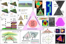
          Graphical abstract

          Related collections

          Most cited references195

          • Record: found
          • Abstract: found
          • Article: not found

          Deep learning.

          Deep learning allows computational models that are composed of multiple processing layers to learn representations of data with multiple levels of abstraction. These methods have dramatically improved the state-of-the-art in speech recognition, visual object recognition, object detection and many other domains such as drug discovery and genomics. Deep learning discovers intricate structure in large data sets by using the backpropagation algorithm to indicate how a machine should change its internal parameters that are used to compute the representation in each layer from the representation in the previous layer. Deep convolutional nets have brought about breakthroughs in processing images, video, speech and audio, whereas recurrent nets have shone light on sequential data such as text and speech.
            Bookmark
            • Record: found
            • Abstract: found
            • Article: not found

            Electric Field Effect in Atomically Thin Carbon Films

            We describe monocrystalline graphitic films, which are a few atoms thick but are nonetheless stable under ambient conditions, metallic, and of remarkably high quality. The films are found to be a two-dimensional semimetal with a tiny overlap between valence and conductance bands, and they exhibit a strong ambipolar electric field effect such that electrons and holes in concentrations up to 10 13 per square centimeter and with room-temperature mobilities of ∼10,000 square centimeters per volt-second can be induced by applying gate voltage.
              Bookmark
              • Record: found
              • Abstract: found
              • Article: not found

              Single-layer MoS2 transistors.

              Two-dimensional materials are attractive for use in next-generation nanoelectronic devices because, compared to one-dimensional materials, it is relatively easy to fabricate complex structures from them. The most widely studied two-dimensional material is graphene, both because of its rich physics and its high mobility. However, pristine graphene does not have a bandgap, a property that is essential for many applications, including transistors. Engineering a graphene bandgap increases fabrication complexity and either reduces mobilities to the level of strained silicon films or requires high voltages. Although single layers of MoS(2) have a large intrinsic bandgap of 1.8 eV (ref. 16), previously reported mobilities in the 0.5-3 cm(2) V(-1) s(-1) range are too low for practical devices. Here, we use a halfnium oxide gate dielectric to demonstrate a room-temperature single-layer MoS(2) mobility of at least 200 cm(2) V(-1) s(-1), similar to that of graphene nanoribbons, and demonstrate transistors with room-temperature current on/off ratios of 1 × 10(8) and ultralow standby power dissipation. Because monolayer MoS(2) has a direct bandgap, it can be used to construct interband tunnel FETs, which offer lower power consumption than classical transistors. Monolayer MoS(2) could also complement graphene in applications that require thin transparent semiconductors, such as optoelectronics and energy harvesting.
                Bookmark

                Author and article information

                Contributors
                Journal
                iScience
                iScience
                iScience
                Elsevier
                2589-0042
                19 February 2022
                18 March 2022
                19 February 2022
                : 25
                : 3
                : 103942
                Affiliations
                [1 ]Materials Science Centre, Quantum Materials and Device Research Laboratory, Indian Institute of Technology Kharagpur, Kharagpur, West Bengal, India
                [2 ]Department of Microtechnology and Nanoscience, Quantum Device Physics Laboratory, Chalmers University of Technology, Göteborg, Sweden
                Author notes
                []Corresponding author saroj.dash@ 123456chalmers.se
                [∗∗ ]Corresponding author prasana@ 123456matsc.iitkgp.ac.in
                Article
                S2589-0042(22)00212-7 103942
                10.1016/j.isci.2022.103942
                8898921
                35265814
                9d2e57d9-0dd3-4c72-82b6-dc9630c2dc6a
                © 2022 The Author(s)

                This is an open access article under the CC BY-NC-ND license (http://creativecommons.org/licenses/by-nc-nd/4.0/).

                History
                Categories
                Perspective

                materials science,materials synthesis,nanomaterials
                materials science, materials synthesis, nanomaterials

                Comments

                Comment on this article