6
views
0
recommends
+1 Recommend
1 collections
    0
    shares
      • Record: found
      • Abstract: found
      • Article: found
      Is Open Access

      A route to engineered high aspect-ratio silicon nanostructures through regenerative secondary mask lithography†

      research-article
      , , , , ,
      Nanoscale
      The Royal Society of Chemistry

      Read this article at

      ScienceOpenPublisherPMC
      Bookmark
          There is no author summary for this article yet. Authors can add summaries to their articles on ScienceOpen to make them more accessible to a non-specialist audience.

          Abstract

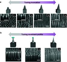
          Silicon nanostructuring imparts unique material properties including antireflectivity, antifogging, anti-icing, self-cleaning, and/or antimicrobial activity. To tune these properties however, a good control over features’ size and shape is essential. Here, a versatile fabrication process is presented to achieve tailored silicon nanostructures (thin/thick pillars, sharp/truncated/re-entrant cones), of pitch down to ∼50 nm, and high-aspect ratio (>10). The approach relies on pre-assembled block copolymer (BCP) micelles and their direct transfer into a glass hard mask of an arbitrary thickness, now enabled by our recently reported regenerative secondary mask lithography. During this pattern transfer, not only can the mask diameter be decreased but also uniquely increased, constituting the first method to achieve such tunability without necessitating a different molecular weight BCP. Consequently, the hard mask modulation (height, diameter) advances the flexibility in attainable inter-pillar spacing, aspect ratios, and re-entrant profiles (= glass on silicon). Combined with adjusted silicon etch conditions, the morphology of nanopatterns can be highly customized. The process control and scalability enable uniform patterning of a 6-inch wafer which is verified through cross-wafer excellent antireflectivity (<5%) and water-repellency (advancing contact angle 158°; hysteresis 1°). The implementation of this approach to silicon nanostructuring is envisioned to be far-reaching, facilitating fundamental studies and targeting applications spanning solar panels, antifogging/antibacterial surfaces, sensing, amongst many others.

          Abstract

          A versatile fabrication platform is presented to achieve tailored silicon nanostructures (pillars, sharp/truncated/re-entrant cones), of pitch down to ∼50 nm, and high-aspect ratio (>10), enabling exceptional tuning of nanopattern-induced properties.

          Related collections

          Author and article information

          Journal
          Nanoscale
          Nanoscale
          NR
          NANOHL
          Nanoscale
          The Royal Society of Chemistry
          2040-3364
          2040-3372
          18 January 2022
          3 February 2022
          18 January 2022
          : 14
          : 5
          : 1847-1854
          Affiliations
          [a] Photonic Innovations Lab, Department of Electronic & Electrical Engineering, University College London Torrington Place London WC1E 7JE UK i.papakonstantinou@ 123456ucl.ac.uk
          [b] Nanoengineered Systems Laboratory, Department of Mechanical Engineering, University College London Torrington Place London WC1E 7JE UK
          [c] Wellcome/EPSRC Centre for Interventional and Surgical Sciences (WEISS), University College London London W1W 7TS UK
          [d] Department of Chemistry, University College London Torrington Place London WC1E 7JE UK
          Author notes
          [‡]

          These authors contributed equally to this work.

          Author information
          https://orcid.org/0000-0003-2910-2767
          https://orcid.org/0000-0001-5143-6881
          https://orcid.org/0000-0002-4072-6610
          https://orcid.org/0000-0002-1087-7020
          Article
          d1nr07024j
          10.1039/d1nr07024j
          9115640
          35040848
          a96f05de-db74-48bd-b30b-426ef65d832b
          This journal is © The Royal Society of Chemistry
          History
          : 23 October 2021
          : 7 January 2022
          Page count
          Pages: 8
          Funding
          Funded by: Engineering and Physical Sciences Research Council, doi 10.13039/501100000266;
          Award ID: EP/N509577/1
          Funded by: Lloyd's Register Foundation, doi 10.13039/100008885;
          Award ID: ICON
          Funded by: H2020 European Research Council, doi 10.13039/100010663;
          Award ID: 679891
          Award ID: 714712
          Categories
          Chemistry
          Custom metadata
          Paginated Article

          Comments

          Comment on this article