2
views
0
recommends
+1 Recommend
0 collections
    0
    shares
      • Record: found
      • Abstract: found
      • Article: found
      Is Open Access

      Conductivity and size quantization effects in semiconductor $$ \delta$$ -layer systems

      research-article

      Read this article at

      Bookmark
          There is no author summary for this article yet. Authors can add summaries to their articles on ScienceOpen to make them more accessible to a non-specialist audience.

          Abstract

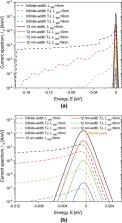
          We present an open-system quantum-mechanical 3D real-space study of the conduction band structure and conductive properties of two semiconductor systems, interesting for their beyond-Moore and quantum computing applications: phosphorus \documentclass[12pt]{minimal} \usepackage{amsmath} \usepackage{wasysym} \usepackage{amsfonts} \usepackage{amssymb} \usepackage{amsbsy} \usepackage{mathrsfs} \usepackage{upgreek} \setlength{\oddsidemargin}{-69pt} \begin{document}$$\delta$$\end{document} -layers and P \documentclass[12pt]{minimal} \usepackage{amsmath} \usepackage{wasysym} \usepackage{amsfonts} \usepackage{amssymb} \usepackage{amsbsy} \usepackage{mathrsfs} \usepackage{upgreek} \setlength{\oddsidemargin}{-69pt} \begin{document}$$\delta$$\end{document} -layer tunnel junctions in silicon. In order to evaluate size quantization effects on the conductivity, we consider two principal cases: nanoscale finite-width structures, used in transistors, and infinitely-wide structures, electrical properties of which are typically known experimentally. For devices widths \documentclass[12pt]{minimal} \usepackage{amsmath} \usepackage{wasysym} \usepackage{amsfonts} \usepackage{amssymb} \usepackage{amsbsy} \usepackage{mathrsfs} \usepackage{upgreek} \setlength{\oddsidemargin}{-69pt} \begin{document}$$W<10$$\end{document}  nm, quantization effects are strong and it is shown that the number of propagating modes determines not only the conductivity, but the distinctive spatial distribution of the current-carrying electron states. For \documentclass[12pt]{minimal} \usepackage{amsmath} \usepackage{wasysym} \usepackage{amsfonts} \usepackage{amssymb} \usepackage{amsbsy} \usepackage{mathrsfs} \usepackage{upgreek} \setlength{\oddsidemargin}{-69pt} \begin{document}$$W>10$$\end{document}  nm, the quantization effects practically vanish and the conductivity tends to the infinitely-wide device values. For tunnel junctions, two distinct conductivity regimes are predicted due to the strong conduction band quantization.

          Related collections

          Most cited references36

          • Record: found
          • Abstract: not found
          • Article: not found

          Self-interaction correction to density-functional approximations for many-electron systems

            Bookmark
            • Record: found
            • Abstract: found
            • Article: not found

            A single-atom transistor.

            The ability to control matter at the atomic scale and build devices with atomic precision is central to nanotechnology. The scanning tunnelling microscope can manipulate individual atoms and molecules on surfaces, but the manipulation of silicon to make atomic-scale logic circuits has been hampered by the covalent nature of its bonds. Resist-based strategies have allowed the formation of atomic-scale structures on silicon surfaces, but the fabrication of working devices-such as transistors with extremely short gate lengths, spin-based quantum computers and solitary dopant optoelectronic devices-requires the ability to position individual atoms in a silicon crystal with atomic precision. Here, we use a combination of scanning tunnelling microscopy and hydrogen-resist lithography to demonstrate a single-atom transistor in which an individual phosphorus dopant atom has been deterministically placed within an epitaxial silicon device architecture with a spatial accuracy of one lattice site. The transistor operates at liquid helium temperatures, and millikelvin electron transport measurements confirm the presence of discrete quantum levels in the energy spectrum of the phosphorus atom. We find a charging energy that is close to the bulk value, previously only observed by optical spectroscopy.
              Bookmark
              • Record: found
              • Abstract: not found
              • Article: not found

              A two-qubit gate between phosphorus donor electrons in silicon

                Bookmark

                Author and article information

                Contributors
                jpmende@sandia.gov
                mamaluy@sandia.gov
                Journal
                Sci Rep
                Sci Rep
                Scientific Reports
                Nature Publishing Group UK (London )
                2045-2322
                30 September 2022
                30 September 2022
                2022
                : 12
                : 16397
                Affiliations
                GRID grid.474520.0, ISNI 0000000121519272, Sandia National Laboratories, ; Albuquerque, NM 87123 USA
                Article
                20105
                10.1038/s41598-022-20105-x
                9525305
                36180529
                a3f81d24-bbd0-434c-8cf0-aa214a213452
                © The Author(s) 2022

                Open AccessThis article is licensed under a Creative Commons Attribution 4.0 International License, which permits use, sharing, adaptation, distribution and reproduction in any medium or format, as long as you give appropriate credit to the original author(s) and the source, provide a link to the Creative Commons licence, and indicate if changes were made. The images or other third party material in this article are included in the article's Creative Commons licence, unless indicated otherwise in a credit line to the material. If material is not included in the article's Creative Commons licence and your intended use is not permitted by statutory regulation or exceeds the permitted use, you will need to obtain permission directly from the copyright holder. To view a copy of this licence, visit http://creativecommons.org/licenses/by/4.0/.

                History
                : 14 June 2022
                : 8 September 2022
                Funding
                Funded by: Laboratory Directed Research and Development
                Award ID: Project No. 227155
                Categories
                Article
                Custom metadata
                © The Author(s) 2022

                Uncategorized
                electronic devices,electronic and spintronic devices,quantum simulation
                Uncategorized
                electronic devices, electronic and spintronic devices, quantum simulation

                Comments

                Comment on this article