13
views
0
recommends
+1 Recommend
0 collections
    0
    shares
      • Record: found
      • Abstract: found
      • Article: found
      Is Open Access

      Cascade synthesis and optoelectronic applications of intermediate bandgap Cu 3VSe 4 nanosheets

      research-article

      Read this article at

      Bookmark
          There is no author summary for this article yet. Authors can add summaries to their articles on ScienceOpen to make them more accessible to a non-specialist audience.

          Abstract

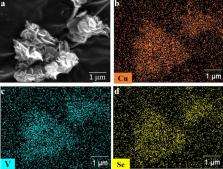
          Two-dimensional (2D) ternary materials recently generated interest in optoelectronics and energy-related applications, alongside their binary counterparts. To date, only a few naturally occurring layered 2D ternary materials have been explored. The plethora of benefits owed to reduced dimensionality prompted exploration of expanding non-layered ternary chalcogenides into the 2D realm. This work presents a templating method that uses 2D transition metal dichalcogenides as initiators to be converted into the corresponding ternary chalcogenide upon addition of copper, via a solution-phase synthesis, conducted in high boiling point solvents. The process starts with preparation of VSe 2 nanosheets, which are next converted into Cu 3VSe 4 sulvanite nanosheets (NSs) which retain the 2D geometry while presenting an X-ray diffraction pattern identical with the one for the bulk Cu 3VSe 4. Both the scanning electron microscopy and transmission microscopy electron microscopy show the presence of quasi-2D morphology. Recent studies of the sulfur-containing sulvanite Cu 3VS 4 highlight the presence of an intermediate bandgap, associated with enhanced photovoltaic (PV) performance. The Cu 3VSe 4 nanosheets reported herein exhibit multiple UV–Vis absorption peaks, related to the intermediate bandgaps similar to Cu 3VS 4 and Cu 3VSe 4 nanocrystals. To test the potential of Cu 3VSe 4 NSs as an absorber for solar photovoltaic devices, Cu 3VSe 4 NSs thin-films deposited on FTO were subjected to photoelectrochemical testing, showing p-type behavior and stable photocurrents of up to ~ 0.036 mA/cm 2. The photocurrent shows a ninefold increase in comparison to reported performance of Cu 3VSe 4 nanocrystals. This proves that quasi-2D sulvanite nanosheets are amenable to thin-film deposition and could show superior PV performance in comparison to nanocrystal thin-films. The obtained electrical impedance spectroscopy signal of the Cu 3VSe NSs-FTO based electrochemical cell fits an equivalent circuit with the circuit elements of solution resistance (R s), charge-transfer resistance (R ct), double-layer capacitance (C dl), and Warburg impedance (W). The estimated charge transfer resistance value of 300 Ω cm 2 obtained from the Nyquist plot provides an insight into the rate of charge transfer on the electrode/electrolyte interface.

          Related collections

          Most cited references56

          • Record: found
          • Abstract: found
          • Article: not found

          Electric Field Effect in Atomically Thin Carbon Films

          We describe monocrystalline graphitic films, which are a few atoms thick but are nonetheless stable under ambient conditions, metallic, and of remarkably high quality. The films are found to be a two-dimensional semimetal with a tiny overlap between valence and conductance bands, and they exhibit a strong ambipolar electric field effect such that electrons and holes in concentrations up to 10 13 per square centimeter and with room-temperature mobilities of ∼10,000 square centimeters per volt-second can be induced by applying gate voltage.
            Bookmark
            • Record: found
            • Abstract: found
            • Article: not found

            Electronics and optoelectronics of two-dimensional transition metal dichalcogenides.

            The remarkable properties of graphene have renewed interest in inorganic, two-dimensional materials with unique electronic and optical attributes. Transition metal dichalcogenides (TMDCs) are layered materials with strong in-plane bonding and weak out-of-plane interactions enabling exfoliation into two-dimensional layers of single unit cell thickness. Although TMDCs have been studied for decades, recent advances in nanoscale materials characterization and device fabrication have opened up new opportunities for two-dimensional layers of thin TMDCs in nanoelectronics and optoelectronics. TMDCs such as MoS(2), MoSe(2), WS(2) and WSe(2) have sizable bandgaps that change from indirect to direct in single layers, allowing applications such as transistors, photodetectors and electroluminescent devices. We review the historical development of TMDCs, methods for preparing atomically thin layers, their electronic and optical properties, and prospects for future advances in electronics and optoelectronics.
              Bookmark
              • Record: found
              • Abstract: found
              • Article: not found

              Quantum-sized carbon dots for bright and colorful photoluminescence.

              We report that nanoscale carbon particles (carbon dots) upon simple surface passivation are strongly photoluminescent in both solution and the solid state. The luminescence emission of the carbon dots is stable against photobleaching, and there is no blinking effect. These strongly emissive carbon dots may find applications similar to or beyond those of their widely pursued silicon counterparts.
                Bookmark

                Author and article information

                Contributors
                dradu@fiu.edu
                Journal
                Sci Rep
                Sci Rep
                Scientific Reports
                Nature Publishing Group UK (London )
                2045-2322
                10 December 2020
                10 December 2020
                2020
                : 10
                : 21679
                Affiliations
                [1 ]GRID grid.65456.34, ISNI 0000 0001 2110 1845, Department of Mechanical and Materials Engineering, , Florida International University, ; Miami, FL 33174 USA
                [2 ]GRID grid.213917.f, ISNI 0000 0001 2097 4943, School of Materials Science and Engineering, , Georgia Institute of Technology, ; Atlanta, GA 30332 USA
                Article
                78649
                10.1038/s41598-020-78649-9
                8097018
                33303797
                720d7c9f-2e17-471e-a0bf-1fac78b3537e
                © The Author(s) 2020

                Open Access This article is licensed under a Creative Commons Attribution 4.0 International License, which permits use, sharing, adaptation, distribution and reproduction in any medium or format, as long as you give appropriate credit to the original author(s) and the source, provide a link to the Creative Commons licence, and indicate if changes were made. The images or other third party material in this article are included in the article's Creative Commons licence, unless indicated otherwise in a credit line to the material. If material is not included in the article's Creative Commons licence and your intended use is not permitted by statutory regulation or exceeds the permitted use, you will need to obtain permission directly from the copyright holder. To view a copy of this licence, visit http://creativecommons.org/licenses/by/4.0/.

                History
                : 1 July 2020
                : 26 November 2020
                Funding
                Funded by: FundRef http://dx.doi.org/10.13039/100000104, National Aeronautics and Space Administration;
                Award ID: 80NSSC19M0201
                Funded by: FundRef http://dx.doi.org/10.13039/100000001, National Science Foundation;
                Award ID: 1924412
                Award Recipient :
                Categories
                Article
                Custom metadata
                © The Author(s) 2020

                Uncategorized
                materials for devices,materials for energy and catalysis,nanoscale materials
                Uncategorized
                materials for devices, materials for energy and catalysis, nanoscale materials

                Comments

                Comment on this article