13
views
0
recommends
+1 Recommend
0 collections
    0
    shares
      • Record: found
      • Abstract: found
      • Article: found
      Is Open Access

      Energy Bandgap and Edge States in an Epitaxially Grown Graphene/ h-BN Heterostructure

      research-article

      Read this article at

      Bookmark
          There is no author summary for this article yet. Authors can add summaries to their articles on ScienceOpen to make them more accessible to a non-specialist audience.

          Abstract

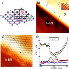
          Securing a semiconducting bandgap is essential for applying graphene layers in switching devices. Theoretical studies have suggested a created bulk bandgap in a graphene layer by introducing an asymmetry between the A and B sub-lattice sites. A recent transport measurement demonstrated the presence of a bandgap in a graphene layer where the asymmetry was introduced by placing a graphene layer on a hexagonal boron nitride ( h-BN) substrate. Similar bandgap has been observed in graphene layers on metal substrates by local probe measurements; however, this phenomenon has not been observed in graphene layers on a near-insulating substrate. Here, we present bulk bandgap-like features in a graphene layer epitaxially grown on an h-BN substrate using scanning tunneling spectroscopy. We observed edge states at zigzag edges, edge resonances at armchair edges, and bandgap-like features in the bulk.

          Related collections

          Most cited references19

          • Record: found
          • Abstract: found
          • Article: found
          Is Open Access

          Half-Metallic Graphene Nanoribbons

          Electrical current can be completely spin polarized in a class of materials known as half-metals, as a result of the coexistence of metallic nature for electrons with one spin orientation and insulating for electrons with the other. Such asymmetric electronic states for the different spins have been predicted for some ferromagnetic metals - for example, the Heusler compounds- and were first observed in a manganese perovskite. In view of the potential for use of this property in realizing spin-based electronics, substantial efforts have been made to search for half-metallic materials. However, organic materials have hardly been investigated in this context even though carbon-based nanostructures hold significant promise for future electronic device. Here we predict half-metallicity in nanometre-scale graphene ribbons by using first-principles calculations. We show that this phenomenon is realizable if in-plane homogeneous electric fields are applied across the zigzag-shaped edges of the graphene nanoribbons, and that their magnetic property can be controlled by the external electric fields. The results are not only of scientific interests in the interplay between electric fields and electronic spin degree of freedom in solids but may also open a new path to explore spintronics at nanometre scale, based on graphene.
            Bookmark
            • Record: found
            • Abstract: found
            • Article: found
            Is Open Access

            Energy Gaps in Graphene Nanoribbons

            Based on a first-principles approach, we present scaling rules for the band gaps of graphene nanoribbons (GNRs) as a function of their widths. The GNRs considered have either armchair or zigzag shaped edges on both sides with hydrogen passivation. Both varieties of ribbons are shown to have band gaps. This differs from the results of simple tight-binding calculations or solutions of the Dirac's equation based on them. Our {\it ab initio} calculations show that the origin of energy gaps for GNRs with armchair shaped edges arises from both quantum confinement and the crucial effect of the edges. For GNRs with zigzag shaped edges, gaps appear because of a staggered sublattice potential on the hexagonal lattice due to edge magnetization. The rich gap structure for ribbons with armchair shaped edges is further obtained analytically including edge effects. These results reproduce our {\it ab initio} calculation results very well.
              Bookmark
              • Record: found
              • Abstract: found
              • Article: not found

              Epitaxial growth of single-domain graphene on hexagonal boron nitride.

              Hexagonal boron nitride (h-BN) has recently emerged as an excellent substrate for graphene nanodevices, owing to its atomically flat surface and its potential to engineer graphene's electronic structure. Thus far, graphene/h-BN heterostructures have been obtained only through a transfer process, which introduces structural uncertainties due to the random stacking between graphene and h-BN substrate. Here we report the epitaxial growth of single-domain graphene on h-BN by a plasma-assisted deposition method. Large-area graphene single crystals were successfully grown for the first time on h-BN with a fixed stacking orientation. A two-dimensional (2D) superlattice of trigonal moiré pattern was observed on graphene by atomic force microscopy. Extra sets of Dirac points are produced as a result of the trigonal superlattice potential and the quantum Hall effect is observed with the 2D-superlattice-related feature developed in the fan diagram of longitudinal and Hall resistance, and the Dirac fermion physics near the original Dirac point is unperturbed. The macroscopic epitaxial graphene is in principle limited only by the size of the h-BN substrate and our synthesis method is potentially applicable on other flat surfaces. Our growth approach could thus open new ways of graphene band engineering through epitaxy on different substrates.
                Bookmark

                Author and article information

                Journal
                Sci Rep
                Sci Rep
                Scientific Reports
                Nature Publishing Group
                2045-2322
                09 August 2016
                2016
                : 6
                : 31160
                Affiliations
                [1 ]Department of Physics, Seoul National University , Seoul 151-747, Korea
                [2 ]Department of Physics, Sejong University , Seoul 143-747, Korea
                [3 ]Center for Nanoscale Science and Technology, National Institute of Standards Technology , Gaithersburg, MD 20899, USA
                Author notes
                [*]

                These authors contributed equally to this work.

                Article
                srep31160
                10.1038/srep31160
                4977565
                27503427
                59fbcb11-87ec-4aa7-82d5-06a407d58c7c
                Copyright © 2016, The Author(s)

                This work is licensed under a Creative Commons Attribution 4.0 International License. The images or other third party material in this article are included in the article’s Creative Commons license, unless indicated otherwise in the credit line; if the material is not included under the Creative Commons license, users will need to obtain permission from the license holder to reproduce the material. To view a copy of this license, visit http://creativecommons.org/licenses/by/4.0/

                History
                : 03 November 2015
                : 15 July 2016
                Categories
                Article

                Uncategorized
                Uncategorized

                Comments

                Comment on this article