49
views
0
recommends
+1 Recommend
0 collections
    0
    shares
      • Record: found
      • Abstract: found
      • Article: found
      Is Open Access

      Sub-micron phase coexistence in small-molecule organic thin films revealed by infrared nano-imaging

      research-article

      Read this article at

      Bookmark
          There is no author summary for this article yet. Authors can add summaries to their articles on ScienceOpen to make them more accessible to a non-specialist audience.

          Abstract

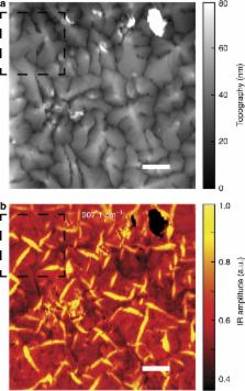
          Controlling the domain size and degree of crystallization in organic films is highly important for electronic applications such as organic photovoltaics, but suitable nanoscale mapping is very difficult. Here we apply infrared-spectroscopic nano-imaging to directly determine the local crystallinity of organic thin films with 20-nm resolution. We find that state-of-the-art pentacene films (grown on SiO 2 at elevated temperature) are structurally not homogeneous but exhibit two interpenetrating phases at sub-micrometre scale, documented by a shifted vibrational resonance. We observe bulk-phase nucleation of distinct ellipsoidal shape within the dominant pentacene thin-film phase and also further growth during storage. A faint topographical contrast as well as X-ray analysis corroborates our interpretation. As bulk-phase nucleation obstructs carrier percolation paths within the thin-film phase, hitherto uncontrolled structural inhomogeneity might have caused conflicting reports about pentacene carrier mobility. Infrared-spectroscopic nano-imaging of nanoscale polymorphism should have many applications ranging from organic nanocomposites to geologic minerals.

          Abstract

          The grain boundaries between two coexisting phases in organic semiconductor pentacene are expected to obstruct charge transport in its thin-film devices. Westermeier et al. use infrared-spectroscopic nano-imaging to show an interlocking morphology, which is uncorrelated with its grain structures.

          Related collections

          Most cited references10

          • Record: found
          • Abstract: found
          • Article: not found

          The path to ubiquitous and low-cost organic electronic appliances on plastic.

          Organic electronics are beginning to make significant inroads into the commercial world, and if the field continues to progress at its current, rapid pace, electronics based on organic thin-film materials will soon become a mainstay of our technological existence. Already products based on active thin-film organic devices are in the market place, most notably the displays of several mobile electronic appliances. Yet the future holds even greater promise for this technology, with an entirely new generation of ultralow-cost, lightweight and even flexible electronic devices in the offing, which will perform functions traditionally accomplished using much more expensive components based on conventional semiconductor materials such as silicon.
            Bookmark
            • Record: found
            • Abstract: found
            • Article: not found

            A general relationship between disorder, aggregation and charge transport in conjugated polymers.

            Conjugated polymer chains have many degrees of conformational freedom and interact weakly with each other, resulting in complex microstructures in the solid state. Understanding charge transport in such systems, which have amorphous and ordered phases exhibiting varying degrees of order, has proved difficult owing to the contribution of electronic processes at various length scales. The growing technological appeal of these semiconductors makes such fundamental knowledge extremely important for materials and process design. We propose a unified model of how charge carriers travel in conjugated polymer films. We show that in high-molecular-weight semiconducting polymers the limiting charge transport step is trapping caused by lattice disorder, and that short-range intermolecular aggregation is sufficient for efficient long-range charge transport. This generalization explains the seemingly contradicting high performance of recently reported, poorly ordered polymers and suggests molecular design strategies to further improve the performance of future generations of organic electronic materials.
              Bookmark
              • Record: found
              • Abstract: found
              • Article: not found

              Flexible organic transistors and circuits with extreme bending stability.

              Flexible electronic circuits are an essential prerequisite for the development of rollable displays, conformable sensors, biodegradable electronics and other applications with unconventional form factors. The smallest radius into which a circuit can be bent is typically several millimetres, limited by strain-induced damage to the active circuit elements. Bending-induced damage can be avoided by placing the circuit elements on rigid islands connected by stretchable wires, but the presence of rigid areas within the substrate plane limits the bending radius. Here we demonstrate organic transistors and complementary circuits that continue to operate without degradation while being folded into a radius of 100 μm. This enormous flexibility and bending stability is enabled by a very thin plastic substrate (12.5 μm), an atomically smooth planarization coating and a hybrid encapsulation stack that places the transistors in the neutral strain position. We demonstrate a potential application as a catheter with a sheet of transistors and sensors wrapped around it that enables the spatially resolved measurement of physical or chemical properties inside long, narrow tubes.
                Bookmark

                Author and article information

                Journal
                Nat Commun
                Nat Commun
                Nature Communications
                Nature Pub. Group
                2041-1723
                11 June 2014
                : 5
                : 4101
                Affiliations
                [1 ]Fakultät für Physik and Center for NanoScience (CeNS), Ludwig-Maximilians-Universität München , Geschwister-Scholl-Platz 1, 80539 München, Germany
                [2 ]Nanosystems Initiative Munich , Schellingstrasse 4, 80799 München, Germany
                [3 ]Neaspec GmbH , Bunsenstrasse 5, 82152 Martinsried, Germany
                Author notes
                Article
                ncomms5101
                10.1038/ncomms5101
                4082641
                24916130
                120ab2dd-f8da-4875-9748-c62c89d9df22
                Copyright © 2014, Nature Publishing Group, a division of Macmillan Publishers Limited. All Rights Reserved.

                This work is licensed under a Creative Commons Attribution-NonCommercial-ShareAlike 4.0 International License. The images or other third party material in this article are included in the article's Creative Commons license, unless indicated otherwise in the credit line; if the material is not included under the Creative Commons license, users will need to obtain permission from the license holder to reproduce the material. To view a copy of this license, visit http://creativecommons.org/licenses/by-nc-sa/4.0/

                History
                : 28 February 2014
                : 13 May 2014
                Categories
                Article

                Uncategorized
                Uncategorized

                Comments

                Comment on this article