10
views
0
recommends
+1 Recommend
0 collections
    0
    shares
      • Record: found
      • Abstract: found
      • Article: not found

      Atomic Scale Study on Growth and Heteroepitaxy of ZnO Monolayer on Graphene

      rapid-communication

      Read this article at

      ScienceOpenPublisherPMC
      Bookmark
          There is no author summary for this article yet. Authors can add summaries to their articles on ScienceOpen to make them more accessible to a non-specialist audience.

          Abstract

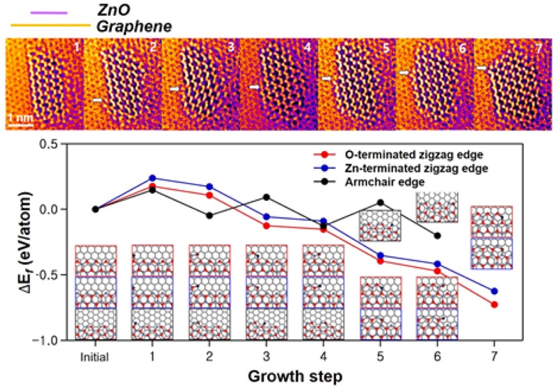
          Atomically thin semiconducting oxide on graphene carries a unique combination of wide band gap, high charge carrier mobility, and optical transparency, which can be widely applied for optoelectronics. However, study on the epitaxial formation and properties of oxide monolayer on graphene remains unexplored due to hydrophobic graphene surface and limits of conventional bulk deposition technique. Here, we report atomic scale study of heteroepitaxial growth and relationship of a single-atom-thick ZnO layer on graphene using atomic layer deposition. We demonstrate atom-by-atom growth of zinc and oxygen at the preferential zigzag edge of a ZnO monolayer on graphene through in situ observation. We experimentally determine that the thinnest ZnO monolayer has a wide band gap (up to 4.0 eV), due to quantum confinement and graphene-like structure, and high optical transparency. This study can lead to a new class of atomically thin two-dimensional heterostructures of semiconducting oxides formed by highly controlled epitaxial growth.

          Related collections

          Most cited references41

          • Record: found
          • Abstract: found
          • Article: found
          Is Open Access

          Ultrahigh electron mobility in suspended graphene

          We have achieved mobilities in excess of 200,000 cm^2/Vs at electron densities of ~2*10^11 cm^-2 by suspending single layer graphene. Suspension ~150 nm above a Si/SiO_2 gate electrode and electrical contacts to the graphene was achieved by a combination of electron beam lithography and etching. The specimens were cleaned in situ by employing current-induced heating, directly resulting in a significant improvement of electrical transport. Concomitant with large mobility enhancement, the widths of the characteristic Dirac peaks are reduced by a factor of 10 compared to traditional, non-suspended devices. This advance should allow for accessing the intrinsic transport properties of graphene.
            Bookmark
            • Record: found
            • Abstract: found
            • Article: not found

            Gate-variable optical transitions in graphene.

            Two-dimensional graphene monolayers and bilayers exhibit fascinating electrical transport behaviors. Using infrared spectroscopy, we find that they also have strong interband transitions and that their optical transitions can be substantially modified through electrical gating, much like electrical transport in field-effect transistors. This gate dependence of interband transitions adds a valuable dimension for optically probing graphene band structure. For a graphene monolayer, it yields directly the linear band dispersion of Dirac fermions, whereas in a bilayer, it reveals a dominating van Hove singularity arising from interlayer coupling. The strong and layer-dependent optical transitions of graphene and the tunability by simple electrical gating hold promise for new applications in infrared optics and optoelectronics.
              Bookmark
              • Record: found
              • Abstract: not found
              • Article: not found

              Zinc oxide nanostructures: growth, properties and applications

              Zhong Wang (2004)
                Bookmark

                Author and article information

                Journal
                Nano Lett
                Nano Lett
                nl
                nalefd
                Nano Letters
                American Chemical Society
                1530-6984
                1530-6992
                06 December 2016
                11 January 2017
                : 17
                : 1
                : 120-127
                Affiliations
                []School of Materials Science and Engineering, Ulsan National Institute of Science and Technology (UNIST) , Ulsan 44919, Republic of Korea
                []School of Energy and Chemical Engineering, Ulsan National Institute of Science and Technology (UNIST) , Ulsan 44919, Republic of Korea
                [§ ]Center for Multidimensional Carbon Materials, Institute for Basic Science (IBS) , Ulsan 44919, Republic of Korea
                []Electron Microscopy Center, Empa − Swiss Federal Laboratories for Materials Science and Technology , CH-8600 Dübendorf, Switzerland
                []Low Dimensional Carbon Material Center, Ulsan National Institute of Science and Technology (UNIST) , Ulsan 44919, Republic of Korea
                Author notes
                [* ](Z.L.) E-mail: zhlee@ 123456unist.ac.kr ).
                Article
                10.1021/acs.nanolett.6b03621
                5238513
                28002942
                ab557f5c-500f-490f-a9fd-fe6e742f29ad
                Copyright © 2016 American Chemical Society

                This is an open access article published under an ACS AuthorChoice License, which permits copying and redistribution of the article or any adaptations for non-commercial purposes.

                History
                : 28 August 2016
                : 06 December 2016
                Categories
                Letter
                Custom metadata
                nl6b03621
                nl-2016-03621m

                Nanotechnology
                heteroepitaxy,atomically thin,2d materials,quantum confinement effect,zno monolayer,graphene

                Comments

                Comment on this article